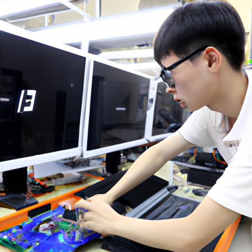
FPGA (Field-Programmable Gate Array) is an integrated circuit that can be programmed by users after manufacturing to achieve different functions. The manufacturing process of FPGA is a complex technology that requires precise equipment and process flow. With the continuous development of technology, the manufacturing process of FPGA is also constantly improving to meet the growing market demand.

1. Design: The manufacturing process of FPGA first requires design. Design engineers design circuit structures and functions that meet the requirements based on user needs and market trends. Design engineers need to consider factors such as circuit layout, connections, and power consumption to ensure the performance and stability of the FPGA.
2. Manufacturing: The manufacturing of FPGA is a complex process involving multiple process steps. The first step is chip manufacturing, which involves using lithography to project circuit patterns onto silicon wafers, followed by etching, deposition, ion implantation, and other steps to form the chip structure. This is followed by packaging and testing, where the chip is packaged in plastic or ceramic packaging and undergoes functional testing and quality inspection.
3. Process Optimization: With the continuous development of technology, the manufacturing process of FPGA is constantly being optimized. For example, using advanced materials and processes can improve the performance and power efficiency of FPGA. In addition, using new design tools and simulation techniques can accelerate the speed of design and verification, reducing time to market for products.
4. Integration: The manufacturing process of FPGA also includes the integration of different functional modules. For example, integrating processor cores, memory, interfaces, and other functions into the same chip to achieve more complex applications. The integration process needs to consider the mutual influence of circuits and the stability of signal transmission to ensure the performance and reliability of the entire system.
In summary, the manufacturing process of FPGA field-programmable gate arrays is a comprehensive process involving design, manufacturing, process optimization, and integration. With the continuous development of technology, the manufacturing process of FPGA is constantly improving to meet the growing market demand. In the future, with the development of emerging technologies such as artificial intelligence and the Internet of Things, the manufacturing process of FPGA will continue to evolve towards higher performance and lower power consumption, providing better solutions for various applications.
FPGA (Field-Programmable Gate Array) is an integrated circuit that can be programmed by users after manufacturing to achieve different functions. The manufacturing process of FPGA is a complex technology that requires precise equipment and process flow. With the continuous development of technology, the manufacturing process of FPGA is also constantly improving to meet the growing market demand.

1. Design: The manufacturing process of FPGA first requires design. Design engineers design circuit structures and functions that meet the requirements based on user needs and market trends. Design engineers need to consider factors such as circuit layout, connections, and power consumption to ensure the performance and stability of the FPGA.
2. Manufacturing: The manufacturing of FPGA is a complex process involving multiple process steps. The first step is chip manufacturing, which involves using lithography to project circuit patterns onto silicon wafers, followed by etching, deposition, ion implantation, and other steps to form the chip structure. This is followed by packaging and testing, where the chip is packaged in plastic or ceramic packaging and undergoes functional testing and quality inspection.
3. Process Optimization: With the continuous development of technology, the manufacturing process of FPGA is constantly being optimized. For example, using advanced materials and processes can improve the performance and power efficiency of FPGA. In addition, using new design tools and simulation techniques can accelerate the speed of design and verification, reducing time to market for products.
4. Integration: The manufacturing process of FPGA also includes the integration of different functional modules. For example, integrating processor cores, memory, interfaces, and other functions into the same chip to achieve more complex applications. The integration process needs to consider the mutual influence of circuits and the stability of signal transmission to ensure the performance and reliability of the entire system.
In summary, the manufacturing process of FPGA field-programmable gate arrays is a comprehensive process involving design, manufacturing, process optimization, and integration. With the continuous development of technology, the manufacturing process of FPGA is constantly improving to meet the growing market demand. In the future, with the development of emerging technologies such as artificial intelligence and the Internet of Things, the manufacturing process of FPGA will continue to evolve towards higher performance and lower power consumption, providing better solutions for various applications.
FPGA (Field-Programmable Gate Array) is an integrated circuit that can be programmed by users after manufacturing to achieve different functions. The manufacturing process of FPGA is a complex technology that requires precise equipment and process flow. With the continuous development of technology, the manufacturing process of FPGA is also constantly improving to meet the growing market demand.

1. Design: The manufacturing process of FPGA first requires design. Design engineers design circuit structures and functions that meet the requirements based on user needs and market trends. Design engineers need to consider factors such as circuit layout, connections, and power consumption to ensure the performance and stability of the FPGA.
2. Manufacturing: The manufacturing of FPGA is a complex process involving multiple process steps. The first step is chip manufacturing, which involves using lithography to project circuit patterns onto silicon wafers, followed by etching, deposition, ion implantation, and other steps to form the chip structure. This is followed by packaging and testing, where the chip is packaged in plastic or ceramic packaging and undergoes functional testing and quality inspection.
3. Process Optimization: With the continuous development of technology, the manufacturing process of FPGA is constantly being optimized. For example, using advanced materials and processes can improve the performance and power efficiency of FPGA. In addition, using new design tools and simulation techniques can accelerate the speed of design and verification, reducing time to market for products.
4. Integration: The manufacturing process of FPGA also includes the integration of different functional modules. For example, integrating processor cores, memory, interfaces, and other functions into the same chip to achieve more complex applications. The integration process needs to consider the mutual influence of circuits and the stability of signal transmission to ensure the performance and reliability of the entire system.
In summary, the manufacturing process of FPGA field-programmable gate arrays is a comprehensive process involving design, manufacturing, process optimization, and integration. With the continuous development of technology, the manufacturing process of FPGA is constantly improving to meet the growing market demand. In the future, with the development of emerging technologies such as artificial intelligence and the Internet of Things, the manufacturing process of FPGA will continue to evolve towards higher performance and lower power consumption, providing better solutions for various applications.
FPGA (Field-Programmable Gate Array) is an integrated circuit that can be programmed by users after manufacturing to achieve different functions. The manufacturing process of FPGA is a complex technology that requires precise equipment and process flow. With the continuous development of technology, the manufacturing process of FPGA is also constantly improving to meet the growing market demand.

1. Design: The manufacturing process of FPGA first requires design. Design engineers design circuit structures and functions that meet the requirements based on user needs and market trends. Design engineers need to consider factors such as circuit layout, connections, and power consumption to ensure the performance and stability of the FPGA.
2. Manufacturing: The manufacturing of FPGA is a complex process involving multiple process steps. The first step is chip manufacturing, which involves using lithography to project circuit patterns onto silicon wafers, followed by etching, deposition, ion implantation, and other steps to form the chip structure. This is followed by packaging and testing, where the chip is packaged in plastic or ceramic packaging and undergoes functional testing and quality inspection.
3. Process Optimization: With the continuous development of technology, the manufacturing process of FPGA is constantly being optimized. For example, using advanced materials and processes can improve the performance and power efficiency of FPGA. In addition, using new design tools and simulation techniques can accelerate the speed of design and verification, reducing time to market for products.
4. Integration: The manufacturing process of FPGA also includes the integration of different functional modules. For example, integrating processor cores, memory, interfaces, and other functions into the same chip to achieve more complex applications. The integration process needs to consider the mutual influence of circuits and the stability of signal transmission to ensure the performance and reliability of the entire system.
In summary, the manufacturing process of FPGA field-programmable gate arrays is a comprehensive process involving design, manufacturing, process optimization, and integration. With the continuous development of technology, the manufacturing process of FPGA is constantly improving to meet the growing market demand. In the future, with the development of emerging technologies such as artificial intelligence and the Internet of Things, the manufacturing process of FPGA will continue to evolve towards higher performance and lower power consumption, providing better solutions for various applications.